
Pull to refresh
Logo
Nanolaser could cut computer energy use in half

Nanolaser could cut computer energy use in half

New Capabilities

DTU's topology-optimized nanolaser brings optical interconnects to the microprocessor

Yesterday: ScienceDaily and tech outlets highlight the nanolaser

Overview

Updated Yesterday

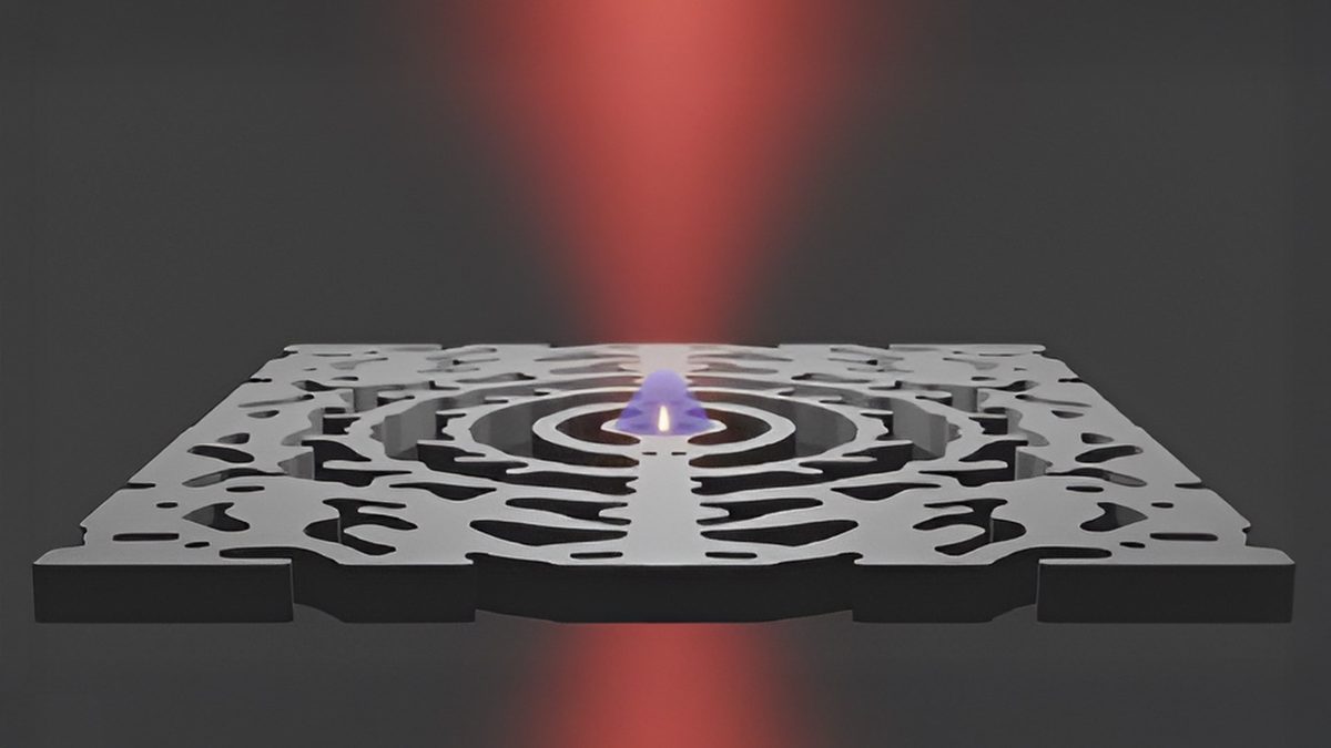
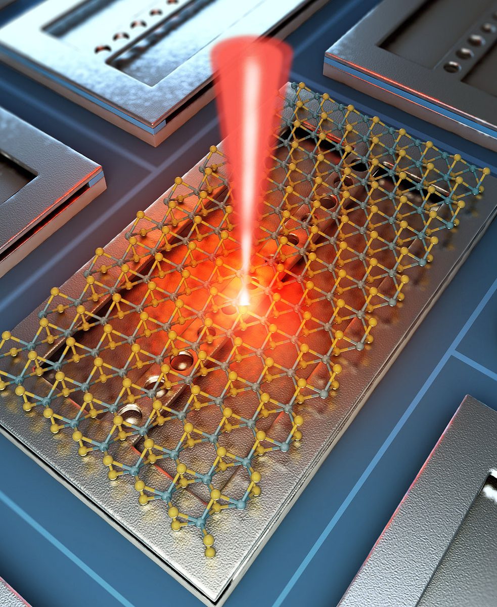
A Danish research team has built a nanolaser small enough that thousands could fit on a single microchip. It traps light in a space far smaller than previous designs and runs at room temperature on very little energy.

Computers still move data inside chips as electrical current, which generates heat and slows performance. Replacing those links with light could reduce a computer's energy use by about half, the researchers estimate. The same shift could shrink power consumption at data centers and support new medical sensors.

Why it matters

If light replaces electricity inside microchips, computers and data centers could run faster while using roughly half today's power.

Questions about this story

Free account needed to ask — your question is kept and asked for you right after sign-up. Answers are public.

No questions yet — be the first to ask.

Key Indicators

50%
Estimated cut in computer energy use
Professor Jesper Mørk's estimate if nanolasers replace electrical interconnects inside chips.
5–10 years
Estimated timeline to electrically pumped nanolaser
Researchers' estimate for solving the remaining electrical-powering challenge, per Mørk.
Room temperature
Operating condition of the nanolaser
The device lasers without cryogenic cooling, a prerequisite for practical chip integration.

Voices

Curated perspectives — historical figures and your fellow readers.

Ever wondered what historical figures would say about today's headlines?

Sign up to generate historical perspectives on this story.

People Involved

Organizations Involved

Timeline

February 2026 September 2026

2 events Latest: Yesterday
  1. ScienceDaily and tech outlets highlight the nanolaser

    Latest Coverage

    The breakthrough reaches wider attention, with Mørk citing 5–10 years to practical electrical versions.

  2. DTU publishes nanolaser research in Science Advances

    Publication

    Team reports a topology-optimized nanolaser, estimating computer energy use could drop by half.

Scenarios

1

Electrically pumped nanolaser demonstrated within five years

Possible Resolves by Sep 11, 2031

Discussed by: DTU researchers, led by Jesper Mørk

Researchers must inject carriers electrically into the optical hotspot of the cavity, the biggest remaining hurdle. Mørk says controlling carrier localization in that hotspot is the central challenge, approached through several methods. Success would open the path to practical on-chip lasers, likely within the five-to-ten-year window he cites.

2

Optical interconnects reach commercial microprocessors

Unlikely Resolves by Sep 11, 2036

Discussed by: Semiconductor industry watchers, chip foundries

Even with a working nanolaser, integration faces coupling losses between laser and waveguide, thermal cycling, control electronics, and fabrication yield. Foundries would need to build thousands of lasers per chip alongside transistors. If adopted, optical links would replace the longest, highest-energy electrical hops inside chips and packages, roughly halving computer power draw as Mørk projects.

3

Nanolaser stays in the lab as integration hurdles persist

Possible Resolves by Sep 11, 2031

Discussed by: Engineering analysis at TechBytes and other technical outlets

Interconnect energy savings depend on system-level factors: what share of chip power is interconnect today, laser and detector efficiency at operating temperature, and conversion overhead at endpoints. Coupling loss between laser, waveguide, and detector often dominates energy more than the laser itself. If any of those stalls, the technology remains a laboratory demonstration rather than a product.

Historical Context

3 moments from history that rhyme with this story — and how they unfolded.

1962

First laser diodes (1962)

Robert Hall at General Electric and Nick Holonyak at GE demonstrated the first injection laser diodes at visible and infrared wavelengths. The devices shrank lasers from room-sized systems to semiconductor chips.

Then

Semiconductor lasers entered products within years, powering optical discs, printers, and later fiber communications.

Now

Every laser that powers today's internet descends from that miniaturization step.

Why this matters now

The nanolaser continues the same arc of miniaturization, compressing the light source to dimensions fit for a single processor core.

1980s–2000s

Optical fiber replaces copper in telecom (1980s–2000s)

Long-distance telecommunications moved from electrical signals in copper cables to light pulses in glass fibers. Bandwidth rose by orders of magnitude, and the economics of carrying data across oceans and continents fundamentally shifted.

Then

Telecom operators built out fiber backbones and submarine cables, enabling the early internet.

Now

Light became the default transport medium for long-distance data, while electricity remained inside computers.

Why this matters now

The DTU nanolaser aims to finish that electrical-to-optical transition, moving the last electrical links inside the chip onto light.

2000s–present

Intel's silicon photonics program (2000s–present)

Intel spent over a decade integrating photonics into silicon, overcoming material mismatches between lasers and silicon waveguides. The program eventually shipped optical transceivers for data centers, but dense on-chip optical links remained out of reach.

Then

Silicon photonics reached the data-center interconnect market for rack-to-rack links.

Now

The program showed both the promise and the difficulty of photonics on silicon: component count, alignment, and thermal management all proved hard to scale.

Why this matters now

The nanolaser targets the same bottleneck Intel chased: tiny, efficient light sources tight enough to sit beside transistors.

Sources

(9)